近日,《Science》刊登了劳伦斯伯克利国家实验室与乔治华盛顿大学等机构合作团队关于半导体合金短程有序的最新研究工作(Science 389, 1342-1346 (2025))。该工作首次在实验中直接捕捉并定量刻画半导体合金中的短程有序(Short-Range Order, SRO),为微电子与量子器件的性能调控开辟了新途径。此次突破得益于能量过滤四维扫描透射电镜(EF-4D-STEM)、GPU 加速高精度机器学习神经演化势函数模型(GPUMD & NEP)与电子衍射模拟(abTEM)的联合应用。
背景
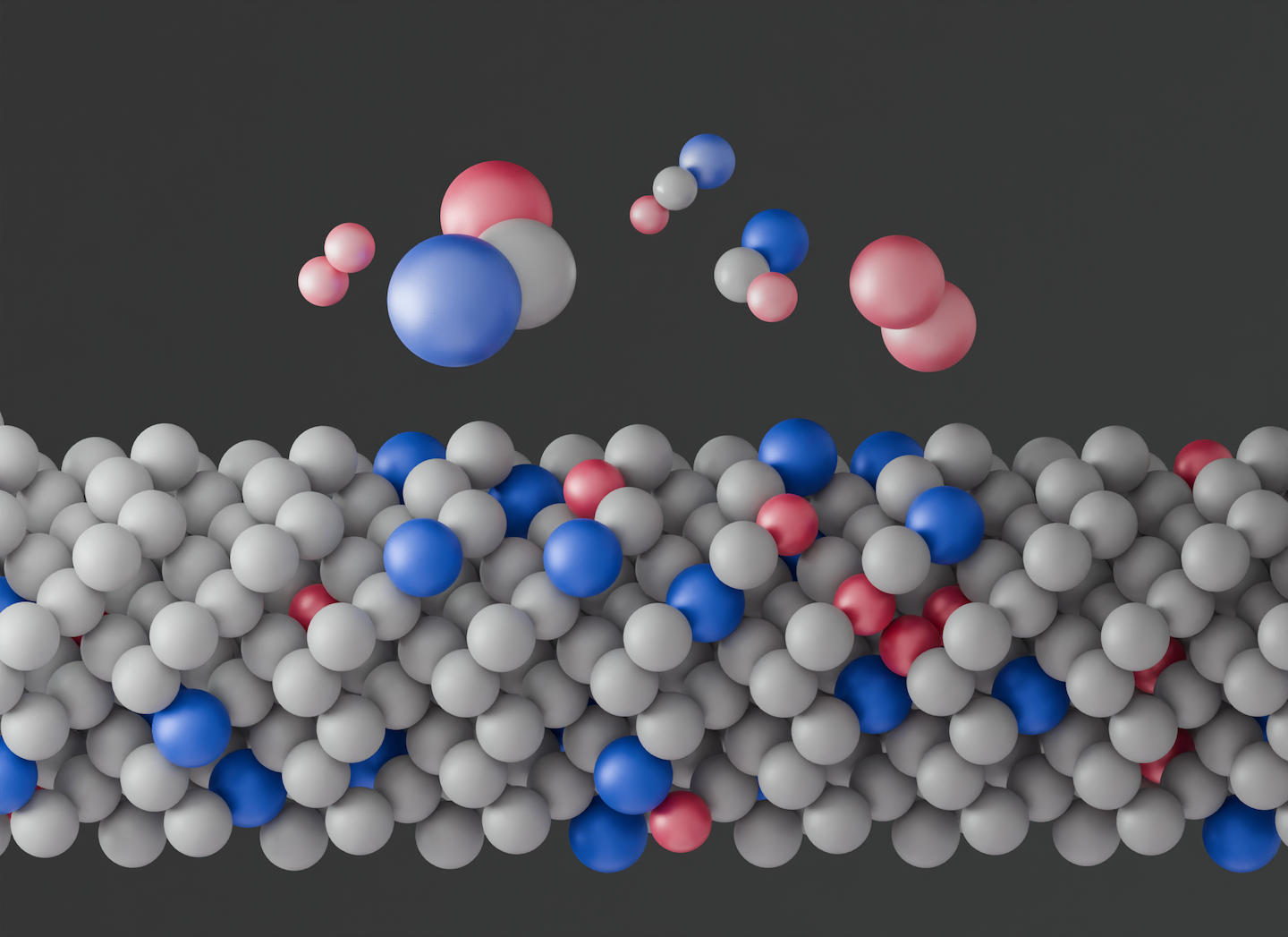
短程有序(SRO)指的是原子在局部近邻范围内存在的统计性排列偏好。通俗地讲,半导体合金材料中的原子并非随机分布,而是在局部形成“朋友圈”——有的原子喜欢“抱团取暖”,而有的却彼此排斥,仿佛“一山不容二虎”。
理论研究表明,这种微妙的局部偏好会影响半导体合金材料的电子能带结构,从而影响材料的性能 [ACS Applied Materials & Interfaces 12, 57245 (2020); Communications Materials 3, 66 (2022); Phys. Rev. Materials 7, L111601 (2023); npj Computational Materials 10, 82 (2024); Phys. Rev. Materials 8, 043805 (2024)]。然而,由于尺度极小且带有统计性特征,科学家们长期以来在实验中一直难以直接观测半导体合金体系中的短程有序。
方法
研究团队以GeSiSn半导体合金为代表体系,结合多种先进实验与模拟方法进行深入研究。GeSiSn半导体合金是一种非常有潜力的硅基微电子、光电子、拓扑量子材料。
-
EF-4D-STEM(能量过滤四维扫描透射电镜): 捕获衍射图像中微弱的弥散散射信号,揭示潜在的 SRO 特征。
-
NEP(Neuroevolution Potential,神经演化势): 兼顾接近第一性原理精度与经典势函数速度的机器学习势函数。[NEP4, Nature Communications 15, 10208 (2024); Chem. Phys. Rev. 6, 011310 (2025)]
-
GPUMD(GPU 加速分子动力学): 将基于NEP 机器学习势函数模型的全原子模拟扩展到百万原子级,生成与实验同尺度的原子模型。[GPUMD 4.0, MGE Advances 3, e70028 (2025)]
-
abTEM: 在大尺度模型上进行电子衍射模拟,与实验数据逐点比对,实现模拟与实验精准对应。[Open Res. Eur. 1, 24 (2021)]
这一整套“实验+模拟组合拳”,实现了百万原子级大规模模拟与实验结果一一对应,使得对原子“朋友圈”(SRO)的精准捕捉成为可能。
结果
- 基于丰富且高质量的第一性原理(DFT)计算训练集,研究团队构建了高精度 NEP 势,并借助 GPUMD 实现了百万原子级 SRO 模型。
- 通过EF-4D-STEM 实验与 abTEM 大尺寸模拟的对比,首次直接确认并定量刻画了 GeSiSn 半导体合金中的短程有序。
- 研究显示,Si-Ge-Sn 三元原子构型是该体系中主导的 SRO 结构,为材料性能调控提供了原子级参考。
意义
- 首次实验验证半导体短程有序,填补长期空白,为能带与电子性质调控提供新途径。
- 展示了NEP 与 GPUMD 在复杂合金材料百万原子级模拟中的可行性与优势。
- SRO 有望成为继成分与应变之外的“第三个自由度”,为下一代微电子、光电器件、量子材料及类脑芯片的设计提供新思路。
展望
未来,科学家或许能像“搭积木”一样,通过设计原子的近邻“朋友圈”(短程有序)来实现材料性能的精细调控。这可能在先进微电子、量子器件、新型光电材料乃至类脑芯片中带来突破。同时,NEP 与 GPUMD 也将在复杂材料的多尺度模拟中发挥更大作用。
论文信息
Lilian M. Vogl, Shunda Chen, Peter Schweizer, Xiaochen Jin, Shui-Qing Yu, Jifeng Liu, Tianshu Li, Andrew M. Minor.
“Identification of short-range ordering motifs in semiconductors”.
Science, 389, 1342–1346 (2025).
全文链接: https://www.science.org/doi/10.1126/science.adu0719
Chemical short-range ordering is expected to be a key factor for tuning the electronic structure of semiconductors. However, experimental evidence of short-range ordering is still lacking due to the challenge of characterizing atomic-scale ordering motifs. Here, we determined the presence of short-range order in a ternary GeSiSn semiconductor system using advanced energy-filtered four-dimensional scanning transmission electron microscopy and large-scale atomistic models generated by a machine learning neuroevolution potential of first-principles accuracy. This approach revealed preferred ordering of different atomic species with the dominant occurrence of Si–Ge–Sn triplets. Our findings not only confirmed the presence of short-range order but also directly revealed the actual atomic structure, demonstrating the potential for informed atomic order–based band engineering as a third degree of freedom beyond composition and strain tuning.
Short-range order (SRO) refers to the tendency of atoms to arrange themselves in a crystal lattice over small distances (typically less than a few nanometers) without forming a fully ordered compound at long ranges. SRO in metals has been linked to properties of mechanical deformation, and in ceramics has been linked to properties related to diffusion. In semiconductors, the concept of SRO has only rarely been studied beyond theoretical predictions linking SRO to important changes in electronic band structure. Using energy-filtered electron microscopy and complementary simulations, Vogl et al. confirmed the presence of SRO in a germanium-silicon-tin semiconductor and identified the actual atomic structure of the SRO motifs. Their work explores an exciting area for understanding and controlling SRO in semiconductors.